Products

Epitaxy process is actually a thin layer single crystal growth technique, which involves growing a new single crystal layer with a certain conductivity type, resistivity, thickness, and lattice structure consistent with bulk single crystals along the crystal direction on the substrate of silicon single crystals under certain conditions.
Item No :
007Order(MOQ) :
1Payment :
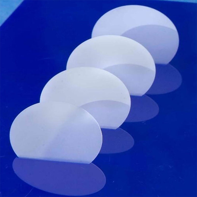
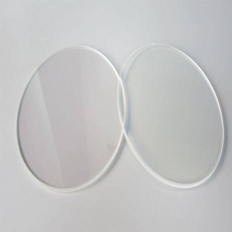
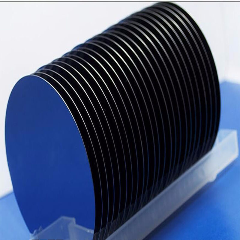
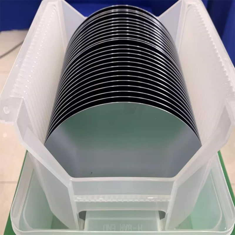
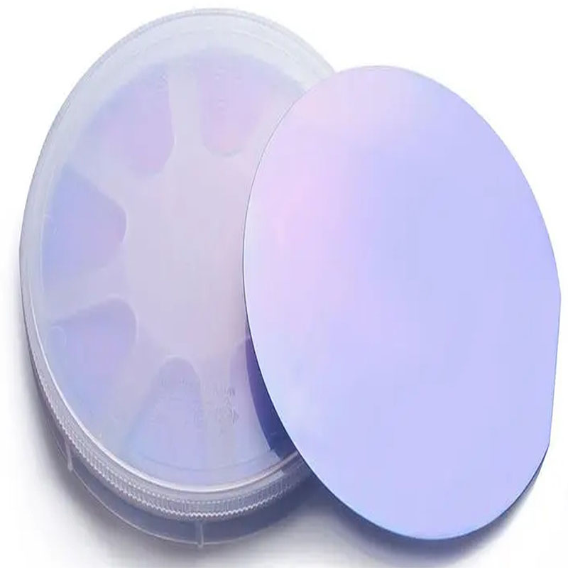
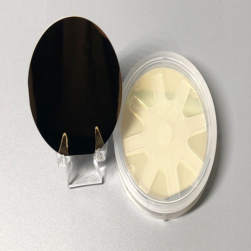
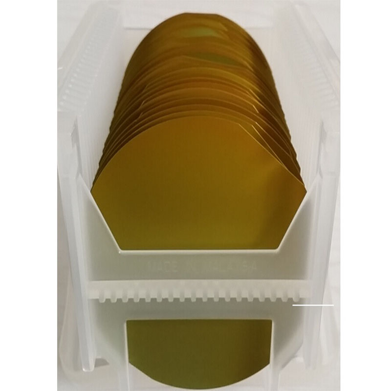
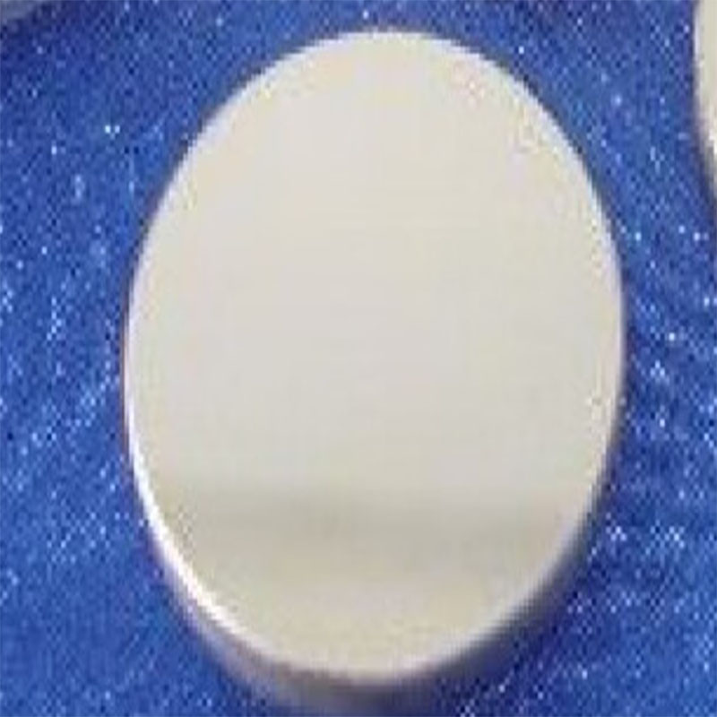
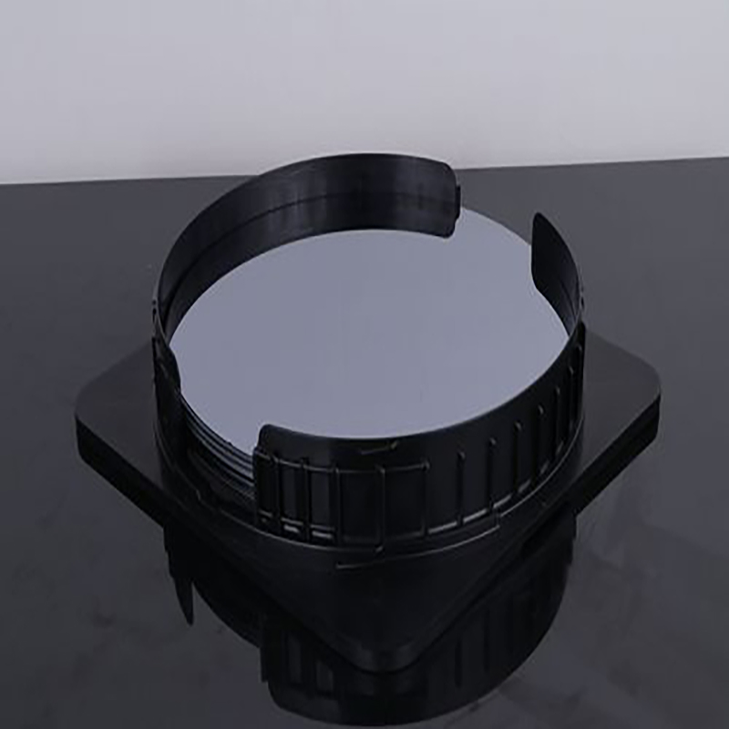
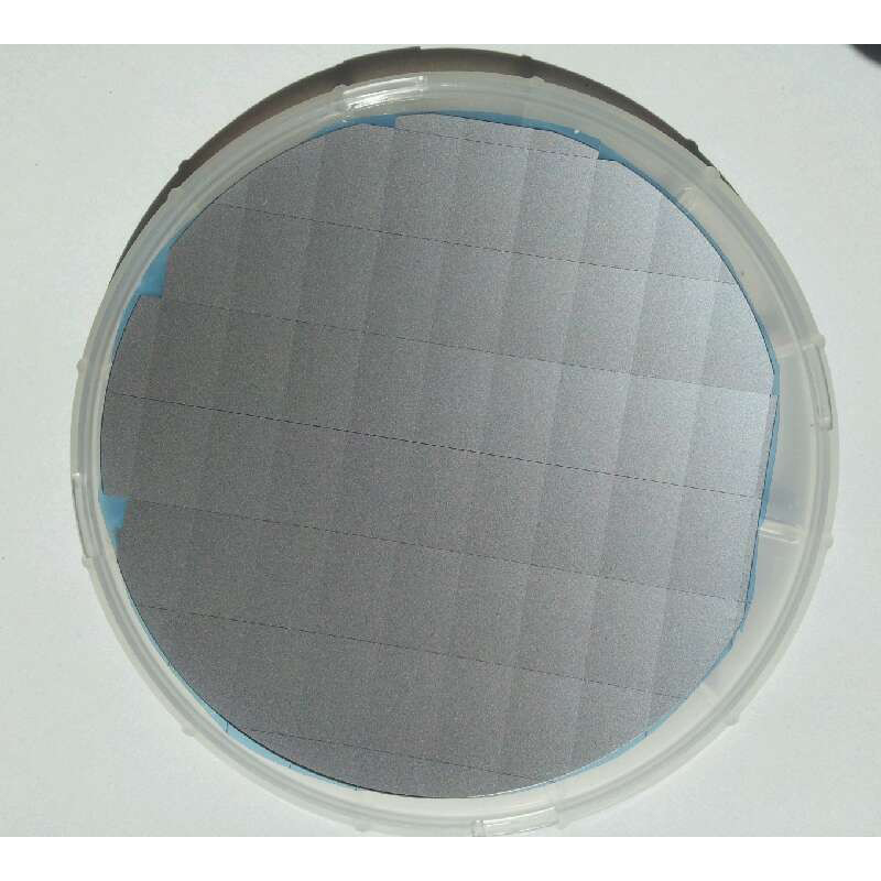
100% PrepayEpitaxial Silicon Wafer
We can supply 3-8inch Epitaxial silicon wafer
Substrate
Type:P,N
Dopant:Boron,Sb,Phos
Thickness:as your request
Resistivity :as your request
Epi layer type :P,P+,N,N+
Thickness of Epi layer:5-100um
The resistivity of Epi laer:0.001-100 Ohm.cm
Note:We can provide customized .Welcome to contact us .
Application:
Silicon epitaxial wafers are a high-quality material commonly used for manufacturing high-end semiconductor devices and integrated circuits. Specific uses include:
1. MOSFET devices with high electron mobility and low noise characteristics
2. High frequency power amplifier, phase-locked loop, and RF front-end components
3. Solar cells
4. LED and laser diode
5. Sensors and power electronic devices operating at high temperatures
6. Optoelectronic devices for high-speed communication equipment
In summary, the application range of silicon epitaxial wafers is very broad, involving multiple fields such as information communication, energy, optoelectronics, etc
FAQ:
1:What's the minimum order quantity ?
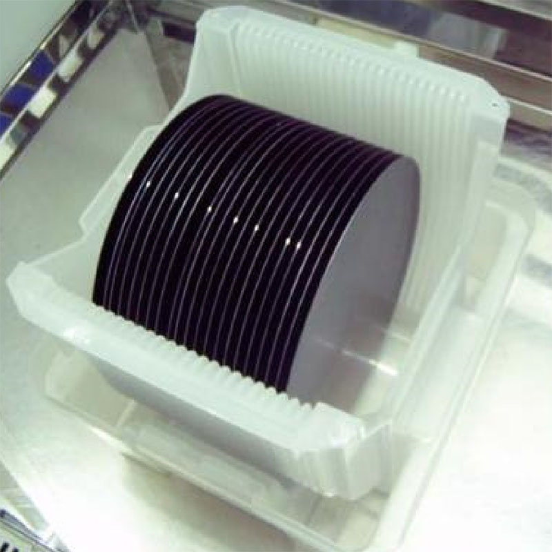
We have stock so please inform the quantity you need and then we will check the quantity of our stock .If we don't have stock will base on our material we have .
2:What's the production time?
If we have stock the lead time around 2-3week .If need make production the lead time need discuss base on your quantity .
3:What is your payment method ?
Usualy by TT if you need other method pls discuss with us .
Subscribe And Save Stay in touch.
Subscribe to get notified about product launches, special offers and news.Address :Room 803, No. 44, Yindou Nanli, Jimei District, Xiamen, China


Link:
Network Card
Nbsmti
huaqingcn
amorphousoem
Reflectop
Copyright 2026@ HC Wafer Semiconductor Material. All Rights Reserved.Sitemap | blog | Xml | Privacy Policy  Network Supported