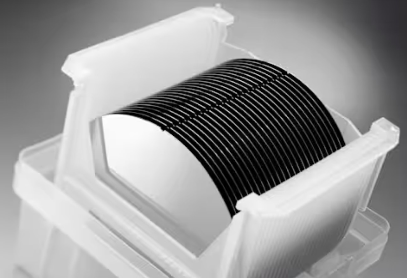
Semiconductor wafer
Dec 03, 2023
According to the classification of manufacturing processes, semiconductor silicon wafers can be mainly divided into polished wafers, epitaxial wafers, and high-end silicon-based materials represented by SOI silicon wafers. Single crystal silicon ingots are processed by cutting, grinding, and polishing to obtain polished wafers. The polished wafer undergoes epitaxial growth to form an epitaxial wafer, which is then processed by processes such as oxidation, bonding, or ion implantation to form an SOI silicon wafer.
According to size classification, the dimensions of semiconductor silicon wafers (calculated in diameter) mainly include specifications such as 125mm (5 inches), 150mm (6 inches), 200mm (8 inches), and 300mm (12 inches).
The larger the size of the silicon wafer, the more chips there are on a single silicon wafer, which can improve production efficiency and reduce production costs. 300mm silicon wafer is 2.25 times the area of 200mm silicon wafer, and in terms of the number of chips produced, 1.5cm × Taking a 1.5cm chip as an example, there are 232 300mm silicon chips and 88 200mm silicon chips. The number of 300mm silicon chips is 2.64 times that of 200mm silicon chips.

![]() Network Supported
Network Supported