Blog

Home

Blog

  • Main Classification of Semiconductor Materials
    Main Classification of Semiconductor Materials Sep 28, 2023
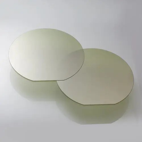
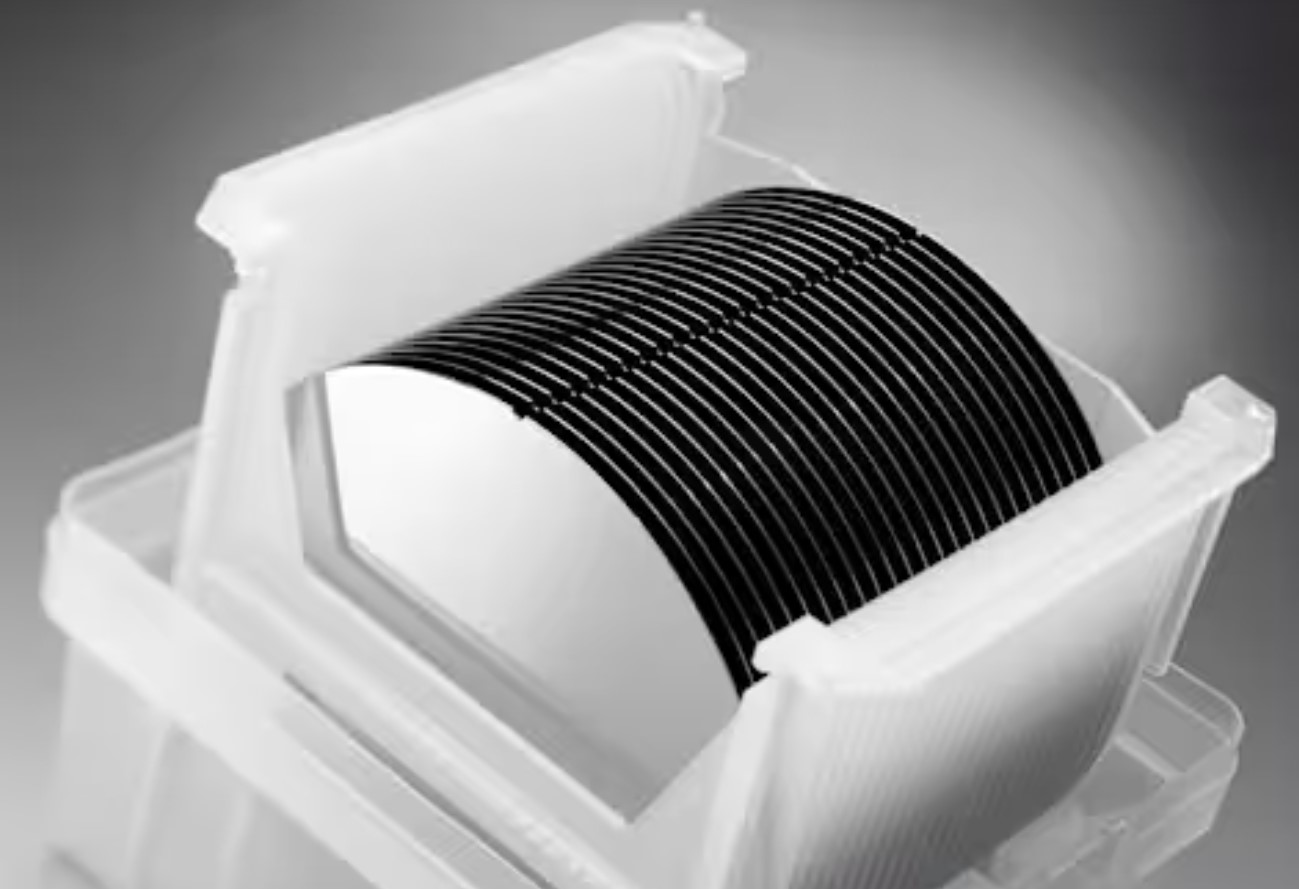
    Semiconductor materials are divided according to application links and can be divided into two categories: front-end wafer manufacturing materials and back-end packaging materials. The main wafer manufacturing materials include: silicon wafers, electronic special gases, photoresists and supporting reagents, wet electronic chemicals, polishing materials, targets, photomasks, etc.; the main packaging materials include: lead frames, packaging substrates , plastic sealing materials, ceramic materials, bonding wires, cutting materials, etc.   Proportion of various materials:   Among semiconductor materials, manufacturing materials account for approximately 63.1%, and packaging materials account for 36.9%;   Among wafer manufacturing materials, silicon wafers account for the highest proportion, accounting for 35%; electronic gas ranks second, accounting for 13%; masks rank third, accounting for 12%, and photoresist accounts for 6%; photoresist ranks third Supporting materials account for 8%; wet electronic chemicals account for 7%; CMP polishing materials account for 6%; target materials account for 2%.   Among packaging materials, packaging substrates account for the highest proportion at 48%; lead frames, bonding wires, packaging materials, ceramic substrates, and chip bonding materials account for 15%, 15%, 10%, 6%, and 3% .
  • Silicon Wafer In Everywhere Nov 07, 2023
    Silicon wafers are ubiquitous in our lives.   Silicon chips are widely used in computing devices such as personal computers, servers, and supercomputers. They serve as the core of the central processing unit (CPU) and control the operation of the entire computer system. The high integration and performance of silicon chips make computer systems more efficient, stable, and fast. In addition, silicon chips are also used for storage, graphics processing, and control of various input and output devices.   The communication field is also one of the areas where silicon chips are widely used. Modern communication devices such as mobile phones, smartphones, wireless routers, and communication base stations cannot do without silicon chips. Silicon chips control key functions such as wireless communication, signal processing, and data transmission in these devices. With the arrival of the 5G era, the application prospects of silicon chips are becoming more broad. They will undertake more computing and processing tasks, providing guarantees for faster and more stable communication systems.   The field of consumer electronics is also an important application field for silicon chips. Various electronic products in modern life, such as smart televisions, game consoles, cameras, audio playback devices, etc., require silicon chips to achieve various functions. The high performance and low power consumption of silicon chips make these devices more intelligent, portable, and power-saving. In addition, with the rise of artificial intelligence and the Internet of Things, the application of silicon chips in the field of consumer electronics will further expand.   The widespread application of silicon wafers has brought about tremendous changes in our lives.
  • Semiconductor wafer
    Semiconductor wafer Dec 03, 2023
    According to the classification of manufacturing processes, semiconductor silicon wafers can be mainly divided into polished wafers, epitaxial wafers, and high-end silicon-based materials represented by SOI silicon wafers. Single crystal silicon ingots are processed by cutting, grinding, and polishing to obtain polished wafers. The polished wafer undergoes epitaxial growth to form an epitaxial wafer, which is then processed by processes such as oxidation, bonding, or ion implantation to form an SOI silicon wafer. According to size classification, the dimensions of semiconductor silicon wafers (calculated in diameter) mainly include specifications such as 125mm (5 inches), 150mm (6 inches), 200mm (8 inches), and 300mm (12 inches). The larger the size of the silicon wafer, the more chips there are on a single silicon wafer, which can improve production efficiency and reduce production costs. 300mm silicon wafer is 2.25 times the area of 200mm silicon wafer, and in terms of the number of chips produced, 1.5cm × Taking a 1.5cm chip as an example, there are 232 300mm silicon chips and 88 200mm silicon chips. The number of 300mm silicon chips is 2.64 times that of 200mm silicon chips.
  • Zero Diffraction Silicon Wafer For XRD Feb 28, 2024
    Introducing Zero Diffraction Silicon - Redefining Precision in XRD TechnologyStep into the world of cutting-edge X-ray diffraction with Zero Diffraction Silicon. Crafted with meticulous attention to detail, this revolutionary silicon wafer is engineered to eliminate even the slightest hint of diffraction, ensuring accurate and precise results in X-ray diffraction experiments.Unleash the full potential of your XRD system with Zero Diffraction Silicon. As light passes through this remarkable wafer, it encounters no obstacles, no distortions, and no interference. Witness crystal-clear diffraction patterns untouched by the limitations of conventional materials.Designed for perfection, Zero Diffraction Silicon boasts an unmatched level of purity and uniformity. Each wafer is flawlessly fabricated to the highest industry standards, guaranteeing consistency in performance and measurement accuracy. Say goodbye to variation and uncertainty, and embrace the certainty of reliable results.But Zero Diffraction Silicon is not just about unrivaled precision; it also offers exceptional durability. Resistant to temperature fluctuations, chemical reactions, and physical wear, this wafer withstands the most demanding experimental conditions without compromising its phenomenal performance. Be assured of long-lasting quality that serves you through countless experiments.Easy integration is a hallmark of Zero Diffraction Silicon. For seamless setup and operation, the wafer is designed to fit effortlessly into standard XRD systems, eliminating the need for complex modifications or adaptations. This means minimal downtime and maximum productivity, allowing researchers and scientists to focus on what truly matters – pushing the boundaries of scientific discovery.With Zero Diffraction Silicon, a world of possibilities awaits. Unlock the potential of X-ray diffraction with unprecedented accuracy and reliability. Whether exploring new materials, analyzing crystal structures, or studying phase transformations, trust Zero Diffraction Silicon to revolutionize your XRD experiments.Experience the future of XRD technology. Discover Zero Diffraction Silicon today and embrace a new era of precision in scientific research.
  • Differences between 3C SiC, 4H SiC, and 6H SiC May 01, 2024
    Silicon carbide (SiC) wafers are usually single crystals, but these single crystal SiC wafers may be composed of different polycrystalline forms, including 3C SiC, 4H SiC, 6H SiC, etc. Each polycrystalline form has its own unique properties. 3C-SiC has a cubic structure 4H-SiC has a tetragonal structure 6H-SiC has a double hexagonal structure   Their differences in the atomic arrangement pattern and coordination number. 3C-SiC has the highest theoretical electron speed, but also has the largest impurity corrosion traces. 4H-SiC and 6H-SiC have better cost-effectiveness and equipment reliability.   3C-SiC has a cubic crystal structure, with each silicon atom surrounded by four carbon atoms and four adjacent silicon atoms. This structure has the highest theoretical electron speed, but is also susceptible to impurities, leading to impurity corrosion marks.   4H-SiC and 6H-SiC both belong to the hexagonal crystal system. Their atomic arrangements are different, but both have better cost-effectiveness and equipment reliability because their crystal structure has better stability and lower impurity concentrations, allowing them to operate at high temperatures,high power and high voltage conditions.    

Subscribe And Save Stay in touch.

Subscribe to get notified about product launches, special offers and news.
submit

Copyright 2024@ HC Wafer Semiconductor Material. All Rights Reserved.Sitemap | blog | Xml | Privacy Policy Network Supported

leave a message

leave a message
If you are interested in our products and want to know more details,please leave a message here,we will reply you as soon as we can.
submit

home

products

WhatsApp

Contact us